LD3320 Datasheet
Introduction
LD3320 is a "special chip that integrates a speech recognition processor with some external circuits, including AD, DA converters, microphone interface, audio output interface. This chip does not require any external auxiliary chip Flash, RAM, etc., directly integrated in existing products that can do speech recognition / voice / man-machine dialogue function. Further, the identification of a list of key words is any dynamic edited.
Main features are
- Via ICRoute unique fast and stable optimization algorithm, complete the non-specific human speech recognition. Does not require prior training and recording, recognition accuracy rate of 95%.
- Do not need any external auxiliary Flash chip, RAM chips and AD chip, you can complete a language voice recognition function. Truly provides a single-chip speech recognition solutions.
- Each identification may be provided up to 50 candidate recognition sentences, each identification sentence can be a word, phrase, or phrases, the Pinyin string of a length of not more than 10 characters, or 79 bytes. Other hand, discrimination sentence content can be dynamicallyeditorial changes by a system supports a variety of scenes.
- The chip has been prepared within the 16-bit A / D converter, 16-bit D / A converter and amplifier circuit, a microphone, stereo headphones and a mono speaker can be easily connected to the chip pin. Stereo headphone jack of the output power is 20mW, and the speaker interface output power of 550mW, and can produce a clear and loud voice.
- Supports parallel and serial interface, Serial ways to simplify the connection with other modules.
- Can be set to the sleep state, and can be easily activated.
- Supports MP3 playback, without external auxiliary device, the master MCU MP3 data then sent to the LD3320 chip inside can the corresponding PIN output sound from the chip.Product design can choose to get the sound output from the stereo headphones or mono speaker.Support MPEG1 (ISO/IEC11172-3), MPEG2 (ISO/IEC13818-3) and MPEG 2.5 layer 3 and other formats.
- The working power supply of 3.3V, use three AA batteries to meet the power supply needs for portable systems.
Circuit Description
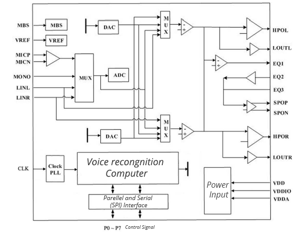
Described in detail as follows:
Voltage requirements
VDD - digital circuit power input - 3.0 V - 3.3 V
VDDIO - digital I / O circuit power input - 1.65 V - VDD
VDDA - analog circuit power input - 3.0 V - 4.0 V
Recommended that the user can use the unified 3.3v voltage input to simplify the design. Digital voltage and analog voltage into
Line isolation can make the chip has a better effect.
Chip pin input voltage range:
A high voltage (logic "1")))): 0.7 * VDDIO ~ VDDIO
A low voltage (logic "0"): 0 ~~ 0.3 * VDDIO
Therefore, developers need to ensure their own master MCU using the same kind of work in 3.3v, master MCU to the LD3320 pin output high voltage does not exceed 3.3V.
Clock (Clock)
The chip must be connected to an external clock, 4-48MHz frequency range is acceptable; while the chip also A PLL frequency synthesizer, a specific frequency can be generated for use by the internal module.
Reset
The chips reset signal (RSTB *) VDD / VDDA / VDDIO stable. No matter what chip ongoing operation, the reset signal can be made to restore the initial state, and each register is reset. If you do not follow the instructions (register settings) after reset chip into hibernation. Since then, a CSB * signal can reactivate the chip to enter the work state.
Parallel Interface
The chip can be connected in parallel and an external host CPU, this time using the eight data lines (P0-P7)and four control signals (WRB *, RDB *, CS *, A0), and an interrupt return signal (INTB *).
Serial Interface
The serial interface is connected via the SPI protocol and external host CPU, First set MD to high, and (SPIS *) ground. Use only four pins: chip select (SCS *), the the the SPI clocks (SDCK) SPI input (SDI) and SPI output (SDO).
Register
Settings and commands on the chip, including the transmit data and receive data, through the operation of the register to complete. For example, voice recognition, set identified a list of key words, setting the recognition mode of the chip, after the recognition is complete guide to the recognition result is accomplished through read / write registers. Play a sound, the MP3 format is the data cycle into the FIFO corresponding to the register. (Recognition result is returned through the register to identify key words arranged in a list of key words serial Index value, the Index value is specified in setting up a list of key words)
The external control of the speaker volume
In addition to specific registers to control the volume, the the chip external circuit can control the speaker volume gain. EP1, EP2, EP3 corresponding pin. See Appendix B
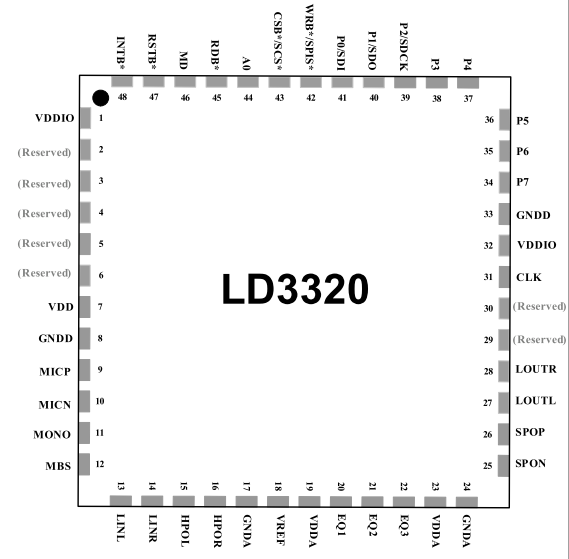
Pins Definitions
| Number | Name | IO Direction | AD type | Descripition |
|---|---|---|---|---|
| 1, 32 | VDDIO | - | - | Digital I / O circuit power input |
| 2 | (Reaserved) | - | - | (Pull-up resistor connected according to the circuit schematic) |
| 3 | (Reaserved) | - | - | (Pull-up resistor connected according to the circuit schematic) |
| 4 | (Reaserved) | - | - | (Pull-up resistor connected according to the circuit schematic) |
| 5 | (Reaserved) | - | - | (Pull-up resistor connected according to the circuit schematic) |
| 6 | (Reaserved) | - | - | Can be null |
| 7 | VDD | - | D | Power or VCC for digital circuit |
| 8, 33 | GNDD | - | D | Ground for IO and digital circuits |
| 9, 10 | MIC[P, N] | I | A | Microphone input (positive and negative terminals) |
| 11 | MONO | I | A | Mono lineIn input |
| 12 | MBS | - | A | Microphone bias |
| 13, 14 | LIN[L, R] | I | A | Stereo LineIn (left and right ends) |
| 15, 16 | HPO[L, R] | O | A | Headphone output (left and right side) |
| 17 | GNDA | - | A | Ground for analog circuit |
| 18 | VREF | - | A | Sound signal reference voltage |
| 19, 23 | VDDA | - | A | VCC for analog circuit |
| 20 | EQ1 | O | A | Speaker volume external control 1 |
| 21 | EQ2 | I | A | Speaker volume external control 2 |
| 22 | EQ3 | O | A | Speaker volume external control 3 |
| 24 | GNDA | - | A | Ground for analog circuit |
| 25, 26 | SPO[N, P] | O | A | Speaker Output |
| 27, 28 | LOUT[L, R] | O | A | LineOut Output |
| 29 | (Reaserved) | - | - | (Refer to Appendix B.4 instructions) |
| 30 | (Reaserved) | - | - | (Refer to Appendix B.4 instructions) |
| 31 | CLK | I | D | Clock input 2-34 (MHz) |
| 34 | P7 | I/O | D | (7) parallel port connection on the pull-up resistor |
| 35 | P6 | I/O | D | (6) parallel port connection on the pull-up resistor |
| 36 | P5 | I/O | D | (5) parallel port connection on the pull-up resistor |
| 37 | P4 | I/O | D | (4) parallel port connection on the pull-up resistor |
| 38 | P3 | I/O | D | (3) parallel port connection on the pull-up resistor |
| 39 | P2/SDCK | I/O | D | (2) Parallel port, shared SPI clock, connect the pull-up resistor |
| 40 | P1/SDO | I/O | D | (1) parallel port, shared SPI output |
| 41 | P0/SDI | I/O | D | Parallel port (0), shared the SPI input, connect the pull-up resistor |
| 42 | WRB*/SPIS* | I | D | Write enable (active low), shared SPI allowing (active low), connect the pull-up resistor |
| 43 | CSB*/SCS* | I | D | Parallel chip select signals, the shared SPI chip select signals connected to the pull-up resistor |
| 44 | A0 | I | D | Address or data selection.WRB * effective, high indicates P0 ~ P7 is the address, while the low P0 ~ P7 data. Pull-up resistors |
| 45 | RDB* | I | D | Reading allows (active low), connect the pull-up resistor |
| 46 | MD | I | D | 0: parallel work, 1: serial work (SPI protocol), connect the pull-up resistor |
| 47 | RSTB* | I | D | Reset signal (active low), connect the pull-up resistor |
| 48 | INTB* | O | D | Interrupt output signal (active low), Connect with Pull-up resistors |
Description:
IO represents direction: I represents input; O represents the output.
AD represents: A represents the analog signal; D represents the digital signal.
The pin distribution as shown below:
Appendix A
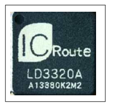
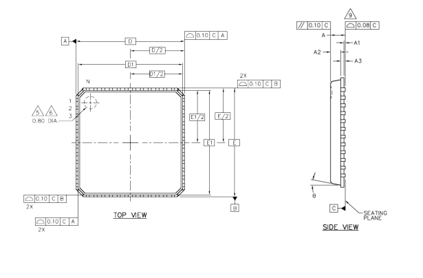
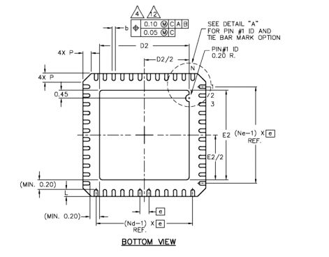
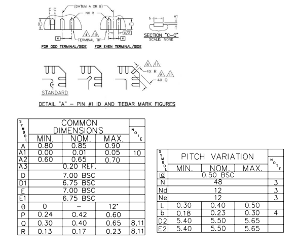
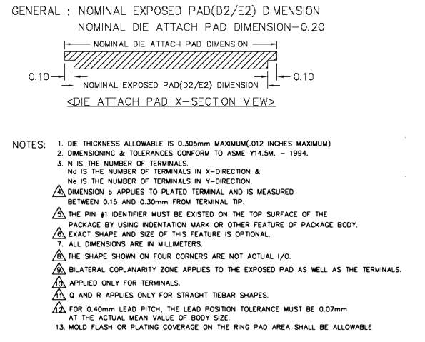
The chip uses a 48-pin QFN plastic package, the size of about 7 * 7 * .85 mm, compact, and pin arrangement is reasonable. Below is the actual image of the front of the package.
Appendix B: Auxiliary circuit
The external control of the speaker volume
The external circuit can change the volume of the speaker, for example, the resistor R6 and the resistance R2 in the following diagram for the 33K and 15K, respectively, then the 33/15 = 2.2, the sound is amplified by about 2 times. If given the variable resistor R6 access, you can manually adjust the volume. Recommends that users adopt a structure similar to the one in Figure B-1 circuit.
The microphone bias of auxiliary circuit
Pin 12 (MBS) is the microphone bias, to pick up an RC circuit can output a floating voltage to the microphone. Recommends that users adopt a structure similar to the one in Figure B-2 circuit.
Correct soldering Pull-up resistors ensure the stable system work
"LD3320 test board schematic gives recommendations on the pull-up resistor, P0 ~ P7, MD, RDB, CSB, INTB, WRB, RSTB, A0 control pins connected to the the 1k/10k upper pull-up resistor, it is recommended that the design try welding pull-up resistor to ensure that the chip control port signal stability, the stability of the auxiliary systems.
Chip analog signal pin needs to correct welding auxiliary circuit
"LD3320 test board schematic gives the periphery of the auxiliary circuits of the chip analog signal pin, including Audio the Input; Audio Output; EQ1/EQ2/EQ3 external speaker volume control circuit; analog power auxiliary circuit. Designers must given according to the schematic diagram of the "LD3320 Beta capacitance / resistance device is properly soldered these auxiliary circuit, in order to ensure that the chip's analog module can work normally.
Chip pin 29, the pin 30 of the instructions
Chip pin 29 and the pin 30, the chip restart after reset (RSTB *), a low output voltage stability. Developers can connect the two pin LED, as shown in the chip power-on indication (such as "LD3320 test board schematic connection). Directly to the two pin vacant.
