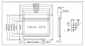
J12864
Reference
Arduino Code
Notes:
- The back of the module comes with 3 * 3 10K hard closure adjustable potentiometer VR1 could be transferred to the desired contrast (the default the 5V factory has good debugging own again adjust the potentiometer for fine tuning, please try to be careful debugging)
- LED backlight polarity adjustable, JP4 LCD backlight plus or minus reverse at
- The module comes with original Samsung genuine anti-static capacitance, anti-interference stronger C6 C7 C8
- serial and parallel two ways to adjust the the PSB interface control two kinds JP2 shorted to P short circuit for the parallel port to the S serial
- Self 3.3V through JP3 adjust the default access + level is 5V, then - is 3.3V, then C4 C5 polar capacitor can model 106A or 104A backlight resistor 33 ohm changed to 3.3 in Europe
Feature
J12864 Chinese character dot matrix LCD display module can display characters and graphics, built-in 8192 Chinese characters (16X16 dot matrix), 128 characters (8X16 lattice) and 64X256 dot matrix display RAM (GDRAM). The main technical parameters and display characteristics:
- Power Supply: VDD 3.3V ~ +5 V (built-in booster circuit, without negative pressure);
- Display: 128 × 64 lines
- Display colors: yellow, and green / blue screen
- Display angle look directly at: 6:00 minutes
- LCD type: STN
- MCU interface: 8-bit or 4-bit parallel / 3 serial
- Configure LED backlight
- A variety of software features: cursor display screen shift, custom characters, sleep mode, etc.
Dimensions
- Dimensions: 93 × 70 × 12.5mm sight size: 73 × 39mm
Pins
| Pins | Name | Direction | Descripition |
|---|---|---|---|
| 1 | GND | - | Power GND |
| 2 | VCC | - | Power VCC |
| 3 | V0 | - | LCD Driver Power VCC |
| 4 | R/S(CS) | H/L | Data selection signal when parallel or chip selection when serial |
| 5 | R/W(SID) | H/L | read or right selection when parallel or data when serial |
| 6 | E(CLK) | H/L | enable when parallel or sync clock when serial |
| 7 | DB0 | H/L | data 0 |
| 8 | DB1 | H/L | data 1 |
| 9 | DB2 | H/L | data 2 |
| 10 | DB3 | H/L | data 3 |
| 11 | DB4 | H/L | data 4 |
| 12 | DB5 | H/L | data 5 |
| 13 | DB6 | H/L | data 6 |
| 14 | DB7 | H/L | data 7 |
| 15 | PSB | H/L | parallel or serial selection, H - parallel, L - serial |
| 16 | NC | Null | |
| 17 | RST | H/L | Reset, enable at low TTL |
| 18 | VOUT | Voltage doubler output pin (VDD = +3.3 V effective) | |
| 19 | LED-A | (LED-5V) | Backlight postive |
| 20 | LED-K | (LED-0V) | Backlight negative |
Timing
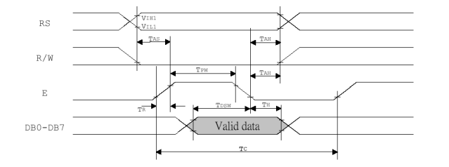
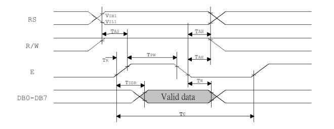
Parallel
Write to module
 Read from module
Serial Timing
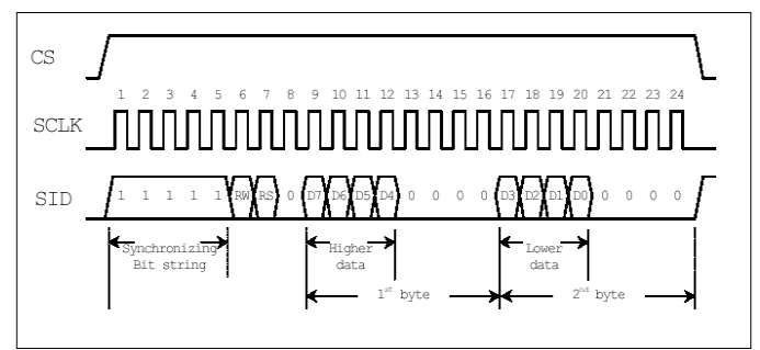
Serial data transfer consists of three bytes to complete:
First byte: serial control - format 11111ABC
- A control for the direction of data transfer: H data from the LCD to the MCU, L data from the MCU to the LCD
- B is a data type selection: H indicates that the data is display data, L represents that the data is a control command
- C is fixed at 0
8-bit data of the second byte: (parallel) 4 - format DDDD0000
Third byte: low 8-bit data (parallel) 4 - format 0000DDDD
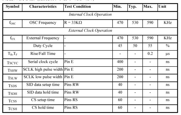
Serial programming reference data
Command list
| Command | RS | RW | DB7 | DB6 | DB5 | DB4 | DB3 | DB2 | DB1 | DB0 | Description | Command Timing (540
KHZ) |
|---|---|---|---|---|---|---|---|---|---|---|---|---|
| Clear Display | 0 | 0 | 0 | 0 | 0 | 0 | 0 | 0 | 0 | 0 | Fill the DDRAM "20H", and set DDRAM address counter (AC) to "00H" | 4.6ms |
| Reset address | 0 | 0 | 0 | 0 | 0 | 1 | S/C | H/L | X | X | Set DDRAM address counter (AC) to "00H", and move the cursor to the beginning of the position of the origin; This command does not change the contents of the DDRAM | 4.6ms |
| enter into point setting mode | 0 | 0 | 0 | 0 | 1 | DL | X | 0RE | X | X | Specified in the read and write data, set the cursor moving direction and specify display shift | 72us |
| Display mode setting | 0 | 0 | 0 | 1 | AC5 | AC4 | AC3 | AC2 | AC1 | AC0 | D = 1: the overall display ON; C = 1: cursor ON; B = 1: cursor position ON | 72us |
| Cursor or display moving control | 0 | 0 | 1 | AC6 | AC5 | AC4 | AC3 | AC2 | AC1 | AC0 | Set cursor moving and display shift control bit; This command does not change the contents of the DDRAM | 72us |
| Function setting | 0 | 0 | 0 | 0 | 1 | DL | X | 0 RE | X | X | DL = 1 (must be set to 1); RE = 1: expansion of the instruction set of actions; RE = 0: The basic instruction set of the action | 72us |
| set CGRAM address | 0 | 0 | 0 | 1 | AC5 | AC4 | AC3 | AC2 | AC1 | AC0 | Set CGRAM address to address counter (AC) | 72us |
| Set DDRAM address | 0 | 0 | 1 | AC6 | AC5 | AC4 | AC3 | AC2 | AC1 | AC0 | Set DDRAM address to address counter (AC) | 0us |
| read busy(BF) sign and address | 0 | 1 | BF | AC6 | AC5 | AC4 | AC3 | AC2 | AC1 | AC0 | Read busy flag (BF) can confirm that the internal operation is completed, the value of the address counter (AC) can be read out | 72us |
| write info into RAM | 1 | 0 | D7 | D6 | D5 | D4 | D3 | D2 | D1 | D0 | Write data to the internal RAM (DDRAM / CGRAM / IRAM / GDRAM) | 72us |
| Read data from RAM | 1 | 1 | D7 | D6 | D5 | D4 | D3 | D2 | D1 | D0 | Read data from the internal RAM (DDRAM / CGRAM / IRAM / GDRAM) | 72us |
| Enter into standby mode | 0 | 0 | 0 | 0 | 0 | 0 | 0 | 0 | 0 | 1 | Fill the DDRAM "20H", and set DDRAM address counter (AC) to "00H" | 72us |
| Roll address or IRAM address selection | 0 | 0 | 0 | 0 | 0 | 0 | 0 | 0 | 0 | SR | Roll address, SR=0 allow input IRAM address | |
| Display reverse selection | 0 | 0 | 0 | 0 | 0 | 0 | 0 | 1 | R1 | R2 | select any row in the four rows to display reverse, and decide if display reverse | 72us |
| Sleep mode selection | 0 | 0 | 0 | 0 | 0 | 0 | 1 | SL | X | X | SL=1, leave sleep mode, SL=0, enter into sleep mode | 72us |
| extended function selection | 0 | 0 | 0 | 0 | 1 | 1 | X | 1 RE | G | 0 | RE=1, extended commands action, RE=0, basic commands action, G=1, drawing display on, g=0, drawing display off | 72us |
| set IRAM address or Roll address | 0 | 0 | 0 | 1 | AC5 | AC4 | AC3 | AC2 | AC1 | AC0 | SR=1, AC5-0 is the vertical rolling address, SR=0, AC3-0 is ICON IRAM address | 72us |
| Set drawing RAM address | 0 | 0 | 1 | AC6 | AC5 | AC4 | AC3 | AC2 | AC1 | AC0 | Set CGRAM set address account (AC) | 72us |
Remarks:
1, when the module before the instruction, microprocessor Shun must make sure that inside the module in a non-busy state BF flag that reads BF needs to 0, before they can receive new instructions; send a command does not check BF flag, then the preceding instruction, and the middle of this command must be delayed for a longer period of time, that is, waiting for the previous instruction does execution completes, the instruction execution time, please refer to the individual instructions in the instruction table instructions.
"Re" is the basic instruction set and expansion instruction set selection control bit, when the "RE" bit is changed, the subsequent instruction set will be maintained in the final state, unless the "RE" is changed again bit, otherwise use the same instruction set, do not need to reset each time the "RE" bit.
