GSM GPRS A6 Module
General Parameters
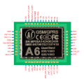
- A6 Dimensions 22.8 × 16.8 × 2.5mm;
- A7 diemsnions: 22.8×19.8×2.5mm;
- Operating temperature -30 ℃ to + 80 ℃;
- Operating Voltage 3.3V-4.2V;
- Power voltage> 3.4V;
- Standby average current 3ma less;
- Support for GSM / GPRS four bands, including 850,900,1800,1900MHZ;
- Support China Mobile and China Unicom's 2G GSM network worldwide;
- GPRS Class 10;
- Sensitivity <-105;
- Support voice calls;
- Support SMS text messaging;
- Support GPRS data traffic, the maximum data rate, download 85.6Kbps, upload 42.8Kbps;
- Supports standard GSM07.07,07.05 AT commands and extended commands Ai-Thinker;
- It supports two serial ports, a serial port to download an AT command port;
- AT command supports the standard AT and TCP / IP command interface;
- Supports digital audio and analog audio support for HR, FR, EFR, AMR speech coding;
- Support ROHS, FCC, CE, CTA certification;
- SMT 42PIN
Main Parameters
- Quad-band 850/900/1800/1900 MHz
- GPRS multi-slot 12, 1 to 12 may be configured
- GPRS mobile station Class B
- Compatible with GSM Phase 2/2 +
- Class 4 (2W @ 850/900 MHz)
- Class 1 (1W @ 1800 / 1900MHz)
- Supply voltage 3.3 ~ 4.2V 4.0V typ.
- Current consumption
- 1.3mA @ DRX = 5
- 1.2mA @ DRX = 9
- Operating temperature -30 ° C to +80 ° C
- Dimensions 22.8 × 16.8 × 2.5mm
- Weight Approximately 3.0g
- AT command control standards GSM07.07,07.05 AT commands and extended commands
- SIM Application Tool Package
Data Transmission
GPRS
- GPRS Class10 up 85.6 kbps (upstream) & 42.8mbps (downlink)
- PBCCH support
- Coding scheme CS 1, 2, 3, 4
- CSD supports up to 14.4 kbps
- Support USSD
- Stack PPP / TCP / UDP / HTTP / FTP / SMTP / MUX
SMS
- To-point messaging
- Cell Broadcast messages
- Text / PDU mode
Voice A speech coding mode:
- Half Rate (HR)
- Full Rate (EFR)
- Enhanced Full Rate (EFR)
AMR:
- Audio processing mechanism
- Echo cancellation
- Echo suppression
- Noise Suppression
Interface
- SIM / USIM card 3V / 1.8V
- UART 2 Ge
- Analog audio interface
- 2 channels (1 channel built Class AB audio amplifier)
- RTC
Certificate
- CE/ FCC/ RoHS/ CTA
Pin Maps
A6 Pin Definitions
| Pin Definition | Pin Definition |
|---|---|
|
|
A20 Pin Definition
| Pin Definition | Pin Definition |
|---|---|
This part pin is Wifi
|
Above pin is wifi
|
A7 Pin Definitions
| Header text | Header text |
|---|---|
|
|
A6C Pin definitions
- Camera interface supports only 30-megapixel fixed-focus camera, the chip can be used include OV7670, GC0308, GC0328, GC0309
| Header text | Header text |
|---|---|
|
|
Quick Start Guide
- Refer to development board
A6
- See the demo video.
- Use Mini Development board, connect VIN, GND, RX and TX, optinally add microUSB power and GSM antenna if the board failed on make calls later
- Connect PWR_KEY to VCC for more than 2 seconds
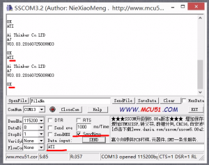
- Open serial monitor set rate 115200, send commands "AT" return "OK"
- Maybe some extra message info:
+CIEV: "MESSAGE",1
+CMT: ,156
0891683110606605F06005800110F00008614011516372238C050003E70202621670B951FB8FDB51650068007400740070003A002F002F007700610070002E00310030003000310030002E0063006F006D002067E58BE28BE660C53002000000000000000000000000000000000000000000000000000000000000000000000000000000000000000000000000000000000000000000000000000000000000000000000000
+CIEV: "MESSAGE",1
+CMT: ,156
0891683110606605F06405800110F00008614011516372238C050003E702016E2999A863D0793AFF1A622A6B620030003467080031003065E50032003465F6FF0C60A85F5367087D2F8BA14F7F75286D4191CF0030002E0030004D0042300251764E2DFF0C770151856D4191CF5DF24F7F75280030002E0030004D0042FF0C52694F59003300300030002E0030004D0042FF1B002056DE590D201C6D4191CF67E58BE2201D
- Or similar like
^CINIT: 1, 0, 0
^CINIT: 1, 0, 0
+CREG: 0
+CREG: 3
- Making phone call, in which 18576608994 is the phone number, and use ATH to hang off the phone call:
ATD18576608994;
A6C Camera
Added AT:
- AT + CAMSTART = N, N from 0-2, N represents the operating mode, 0 QVGA, 1 -VGA, 2-QQVGA
- AT + CAMCAP, take pictures, the default picture format is JPG
- AT + CAMRD, read the contents of the photo is JPG file format
- AT + CAMSTOP, turn off the camera
A7 GPS
Instructions: Increased include AT
- AT + GPS = 1 Open GPS
- AT + GPS = 0 Close GPS
- AT + AGPS = 1 Open AGPS
- AT + AGPS = 0 Close AGPS
- After opening the GPS / AGPS, NEMA default information from GPS_TXD pin output to 9600 baud, if you want NEMA
- From AT serial output, you can use AT + GPSRD.
- AT + GPSRD = 0 Close NEMA output port from the AT
- AT + GPSRD = N NEMA information from AT N seconds once the output port, the actual use of the N into digital;
Other AT commands examples
^CINIT: 2, 32, 41891
^CINIT: 1, 0, 0
^CINIT: 8, 6144, 1
^CINIT: 16, 0, 1638450
^CINIT: 32, 0, 0
+CREG: 0
+CTZV:16/07/06,11:33:25,+08
+CREG: 5

ati                     //check version, manufacturer info
Ai Thinker Co.LTD
A6
V03.03.20160710006H03
OK

at+ccid   //check ccid to see if has sim card
+SCID: SIM Card ID: 898602#4221620070426
OK

at+creg?  //check if network register
+CREG: 1,5
OK

at+csq    //check signal
+CSQ: 31,99
OK

at+cgatt=1          // attached network
+CTZV:16/07/06,11:34:17,+08
OK

at+cgdcont=1,"IP","cmnet"   //set pdp parameter
OK

at+cgact=1,1                 //active this pdp
OK

at+cipstatus?               //check ip connection, should have 8 channels, maxium support 4 channels of tcpip
+CIPSTATUS:0,IP GPRSACT
1,IP INITIAL
2,IP INITIAL
3,IP INITIAL
4,IP INITIAL
5,IP INITIAL
6,IP INITIAL
7,IP INITIAL
OK

at+cipstart="TCP","121.41.97.28",60000   //connect to server
CONNECT OK
OK

at+cipsend=5,qwert    //send 5 bytes, note only support visible characters in this way
OK

at+cipsend=5          //send 5 bytes, send any kind in binary data this way
> ��������
OK

at+cipsend           //send characters, end up with CTRL+Z(hex = 0x1a)
> qwert
�
OK
+CIPRCV:4,test      //receive data 4 bytes from server, content is "test", could be binary data also

at+cipstatus?       //插叙? insert show ip link status
+CIPSTATUS:0,CONNECT OK
1,IP INITIAL
2,IP INITIAL
3,IP INITIAL
4,IP INITIAL
5,IP INITIAL
6,IP INITIAL
7,IP INITIAL
OK

at+cipclose   //close the link
OK

at+cipmux?    //enquiry if multiple link opened查询是否开启多连接
+CIPMUX:0
OK

at+cipmux=1   //turn on multiple link
OK

at+cipstart="TCP","121.41.97.28",60000  //send first TCP connection
+CIPNUM:0                              //only return this when multiple link activated, 0 is the returned link number
CONNECT OK
OK

at+cipstart="TCP","121.41.97.28",60001  //send 2nd TCP connection
+CIPNUM:1                              //only return this when multiple link activated, 1 is the returned link number
CONNECT OK
OK

at+cipstart="TCP","121.41.97.28",60003 //send 3th TCP connection
COMMAND NO RESPONSE!                  //command over time, since the server did not open this port

at+cipstatus?
+CIPSTATUS:0,CONNECT OK
1,CONNECT OK
2,TCP/UDP CONNECTING
3,IP INITIAL
4,IP INITIAL
5,IP INITIAL
6,IP INITIAL
7,IP INITIAL
OK

at+cipclose=3                    //close the connection of link number 3
+CME ERROR:50                    //return error because link no 3. is not established

at+cipclose=2                    //close the connection of link number 2
OK

at+cipstart="TCP","121.41.97.28",60002  //set up new connection
+CIPNUM:2
CONNECT OK
OK

at+cipstart="UDP","121.41.97.28",60006  //setup new udp connection
+CIPNUM:3
UDP BIND OK
OK

at+cipstatus?
+CIPSTATUS:0,CONNECT OK            //can see 0-3 connection are occupied, setup 4 ip connections
1,CONNECT OK
2,CONNECT OK
3,BIND OK
4,IP INITIAL
5,IP INITIAL
6,IP INITIAL
7,IP INITIAL
OK

at+cipsend=0,5,qwert       //link 0 send 5 bytes data “qwert”,this command only support visible data
OK
+CIPRCV:0,4,test           //link 0 receive server data: “test”,this command support any kind of data

at+cipclose=2              //close link 0
OK

at+cipstatus?             //check link info
+CIPSTATUS:0,CONNECT OK
1,CONNECT OK
2,IP CLOSE
3,BIND OK
4,IP INITIAL
5,IP INITIAL
6,IP INITIAL
7,IP INITIAL
OK

at+ciphcfg?              //check heartbeat config
+CIPHCFG:0,10,00,00
1,10,00,00
2,10,00,00
3,10,00,00
4,10,00,00
5,10,00,00
6,10,00,00
7,10,00,00
OK

at+ciphcfg=0,1,112233         //set link 0 heartbeat packet  hex: 0x11,0x22,0x33
OK

at+ciphcfg?
+CIPHCFG:0,10,112233,00
1,10,00,00
2,10,00,00
3,10,00,00
4,10,00,00
5,10,00,00
6,10,00,00
7,10,00,00
OK

at+ciphmode=0,1     //turn on link 0 heartbeat packet
OK

at+cipsend=3,5,qwert    //link 3 send 5 bytes:“qwert”
OK

at+cipclose=3     //close link 3
OK
+TCPCLOSED:1    //server close link 1
OK

at+cipstatus?
+CIPSTATUS:0,CONNECT OK
1,IP CLOSE
2,IP CLOSE
3,IP CLOSE
4,IP INITIAL
5,IP INITIAL
6,IP INITIAL
7,IP INITIAL
OK
+TCPCLOSED:0    //server close link 0
OK

at+cipstatus?
+CIPSTATUS:0,IP CLOSE
1,IP CLOSE
2,IP CLOSE
3,IP CLOSE
4,IP INITIAL
5,IP INITIAL
6,IP INITIAL
7,IP INITIAL
OK
A6 Module
- Connect USB cable and make sure 2A current can be supplied
- Connect any USB-TTL breakout tool, RXD, TXD and GND
- Press Boot button the module will be powered up.
- Turn on serial monitor to send test commands like "AT"
- Example.jpg
Caption2
A20 Module
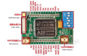
A20 is a GPRS and Wifi Combo module, also supports plug-Camera, Wifi chips with espressif's ESP8285. A20 GPRS part and WIFI part can be separated from a separate power supply, work alone, without disturbing each other. The A20 supports the following modes of operation:
- 1. Separate GPRS mode: In this mode, the user only needs to power on the GPRS alone, and the MCU can control the GPRS part through the serial port.
- 2. Separate WIFI mode: In this mode, the user only needs to power on the WIFI part, and use the MCU to control the WIFI part through the serial port.
- 3. GPRS + WIFI mode: In this mode, the user can use two serial ports to control the GPRS part and WIIF part respectively.
- 4. WIFI master MCU, control GPRS mode: In this mode, the user uses the ESP8285 part of the WIFI as the master, to control the GPRS part, because WIFI is only a two-way serial port, this time the user needs to develop ESP8285 side program;
A20 Breakout
- Toggle 1,3 - GPRS uart port to Pin header,
- Toggle 2,4 - ESP8285 secondary uart port IO13, IO15 to GPRS uart port
- Toggle 5,6 - ESP8285 secondary uart port IO13, IO15 to Pin header
Note of this the breakout board
- DIP switch mark 1 2 3 4 5 6 should be reversed, so if you look on the number mark
toggle 4,6 - turn on GPRS to pin U_TXD and U_RXD
toggle 3,5 - connect  GPRS uart pin to ESP8285 secondary uart port IO13, IO15
toggle 1,2 - Pin header to ESP8285 secondary uart port IO13, IO15
- Wifi Uart pin WRXD, WTXD can always be used, regardless dip switch.
- USB for power ONLY, not for data
Design Note
- The maximum output current of the power supply can not be lower than 2A, otherwise it will be unstable, causing the module to restart;
- Antenna as a result of power, SIM card, serial port will affect the position on the PCB as far as possible, and the best not to the same side of the PCB, if you go 4 layer board, you can string the serial port shielding;
- AT serial port rate is 15200, enter the AT command to \ r \ n end;
- After boot, at to determine whether the module boot,
at + ccid used to determine whether the inserted card or SIM correctly identified to,
at + csq used to query the network signal, generally more than 2,
at + creg? Used to query the network registration 1,1 is a local registration, 1,5 is roaming registration;
Documents
- File:A6 AT commands.pdf
- File:A6 Convert Board 2016031402 V2.pdf
- File:A6 dev board schematic.pdf
- A6C camera capture demo video
- V3 firmware, about how to update please contact us


