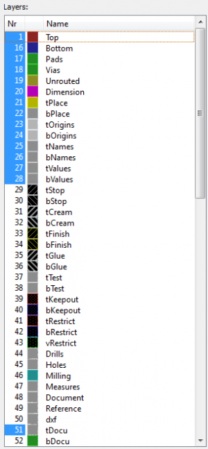
Eagle Layers
Layers in Gerber
| Number | Name | Descrpition |
|---|---|---|
| 1 | Top | topper copper trace |
| 2-15 | Middle | On multi-layer boards with the professional version of Eagle, you also have access to layers 2-15 |
| 16 | Bottom | bottom copper trace |
| 17 | Pads | Normal pads for PTH components (Parts through holes) |
| 18 | Vias | Example (For lines goes from bottom to top or vice verse, help you draw lines easy) |
| 19 | Unrouted | unrouted airwires |
| 20 | Dimension | draw the outline of your PCB on this layer, help the manufacturer to cut it easily, without this outline, it's can't be made. |
| 21 | tPlace | is used to draw lines that will be rendered as the silk screen on your PCBs |
| 22 | bPlace | - |
| 23 | tOrigins | - |
| 24 | bOrigins | - |
| 25 | tNames | is used to hold the unique 'names' for each part on your PCB (ex. C1, R5, X12, etc.) |
| 26 | bNames | - |
| 27 | tValues | is used to hold the value for each part (such as 10K, 0.1µF, AT86RF212, etc.) |
| 28 | bValues | - |
| 51 | tDocu | is used for documentation purposes, such as drawing the mechanical dimensions of your part (more on that shortly!). Normally this layer isn't printed on the PCBs, but it's very important for documentation and for PCB design. |
Setup default layer color
- use script for each design project
- copy and edit mycolor.scr, edit your own color, color number 0 is white in color palette, and same for the rest
Mechanical Layers
All has to be closed loop
- Dimension - 20
- MIlling - 46
