Eagle Design
Design
Setup your environment
In the main windows of eagle, setup the directories in directly setup, library and projects folder are really important from our points of view.
Design a package
- Firstly, you should figure which package you will need. Check in this page.
- In the main window, click new - part library. or double click current library to edit it.
- You should understand the three main important functions here, 1. Make a device, 2. Make a IC package of board design, 3. make a symbol for schemtic, so let's do the 2 & 3 firstly and go 1 at last.
- You can copy the package from other library, just make sure your current part libary is on editing, and open other library in the tree list of eagle main windows, right click, and copy to current part library. Most package you can find at "ref-library.lbr"
- when you are copying the device, the package and symbol will copy together into your new library. And there is no way to copy only symbol I think.
Editing package
- when you are editing the package, make sure the "grid" is turn on, and use 0.005 inches will be a nice choice.
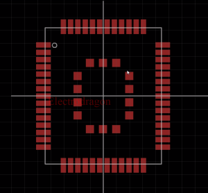
- Draw all kinds of slik screen by using text function, pads or smd for connections, outline for ICs or so.
Drawing symbol
- basically you need to draw a symbol, like a resistor, transitor or so
- add parts name that will display on schematic on it
- add pins by using "pin", the line end WITH the ball should are set to connect to other parts, don't make it vice verse.
- finally add some pin definition to make the device "function" clear.
symmetrical Package
- Normall pins are also symmetrical
- Use 0,0 as center point of package, find +x +y corner
- Draw package outline in on side, mirror x y data to -x -y to other side
- draw pins in certer, change grid to pin pitch
- rename all pads
Connect package and symbol into device
- click the 1 icon for making a final device, click "add" on the left menu to add symbol firstly, and click "new" for package on the left bottom.
- Click connect to connect symbol and package, this is done!
Enabling the Value FieldCreated
If you don't enable this option, all parts will use the device name as the default text for >VALUE, so it's generally a good idea to enable it. There are often variations of packages, and enabling this option allows end users to specify the exact part they intended to use!
Polygon and Gound Fill
- Polygon, for example for power supply net, set:
un-tick thermal
set rank to top 1
normally turn off orphans
set higher isolate to avoid ground or touch.
- For ground fills
turn off orphans
turn off termal
set rank to lowest 6
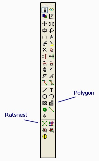
Finally we are to the actual creation of the groundplace itself. This is done by using the Polygon tool in Eagle. Click on the Polygon button and a new menu will popup directly above the pc board layout. This is the parameters that will be used for the polygon that will be drawn on the board. Make sure that the bottom layer is selected, which will be the far left item of the new menu.
Before we draw the polygon, a couple of the default values need to be changed. The width of the line should be changed to 0.010. The Isolate value, which is how much space will be between the groundplace polygon and the other non-grounded elements needs to be selected. On the current version of Eagle it defaults to 0 which is not useful. I select 0.016 or sometimes 0.024 for the Isolate value.
When you have the polygon drawn completely around the perimeter of the circuit, it should look similar to the example here.
The polygon is the blue box just inside the white border of the pcb.
To make the groundplane, we rename the polygon to the same name that is used for the traces connected to the ground pad. If you have changed the name as taught earlier in this article, it will be called GND. To rename the polygon, we go to "Edit" on the top menu, then "Name" from the dropdown list. Now click on the blue polygon line and the box will popup that allows you to enter a new name for the polygon, which we will enter as GND.
There will be another popup box to confirm that you want to connect the polygon to GND, so select it from the choices and hit the OKAY button. The groundplane should automatically fill the bottom layer of the pcb as shown here. You can hit the F2 key to refresh the view and cleanup any stray bits.
If the groundplane does not appear, click the Ratsnest button on the sidebar. Should it still not appear, you likely do not have the polygon and the ground traces using the same name. Did you rename "S1" as instructed in an earlier paragraph?
Note that the pads for all of the components that were connected to ground are now isolated but tied to the groundplane with short copper traces. The components that are not grounded are isolated electrically from the groundplane by a clear space around each pad and trace, which will be the width that was selected in the "Isolate" menu item.
The groundplane does not have to encompass the entire perimeter of the board nor does it even have to be rectangular. Here I have made a small irregular ground fill that just covers the transistor and a few of the component pads. It is not typically done this way on small boards but on larger, more complex layouts this may come in handy.
This type of copper pour is also used to create small heatsink pads on the pcb for transistors or voltage regulators.
