ESP-12F
Datasheet
- CN - https://github.com/Edragon/ai-thinker/blob/main/ESP8266/ESP-12F-01.pdf
- EN - https://github.com/Edragon/ai-thinker/blob/main/ESP8266/ESP-12F-02.pdf
Pin Definition
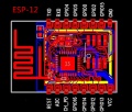
- ESP-12F, ESP-12S
- These two are from ai-thinker, ESP-12S used to be 1MB /8Mbit, now we sell 8MB/32Mbit. Will check this before send to you.
- AI-thinker can check genius via STA MAC address on this link.
ESP-12
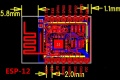
ESP-12 size
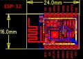
ESP-12 antenna size
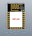
esp12e dimension
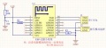
Wiring of ESP-12F


- 1 RST Reset module
- 2 ADC A / D conversion result. The input voltage range is 0 ~ 1V, in the range of 0 ~ 1024
- 3 EN chip enable, high active
- 4 IO16 GPIO16; Wake-up on deep sleep when connected to RST pin.
- 5 IO14 GPIO14; HSPI_CLK
- 6 IO12 GPIO12; HSPI_MISO
- 7 IO13 GPIO13; HSPI_MOSI; UART0_CTS
- 8 VCC 3.3V power supply
- 9 CS0 Chip Select
- 10 MISO Slave Output Host input
- 11 IO9 GPIO9
- 12 IO10 GBIO10
- 13 MOSI Master Output Slave Input
- 14 SCLK clock
- 15 GND GND
- 16 IO15 GPIO15; MTDO; HSPICS; UART0_RTS
- 17 IO2 GPIO2; UART1_TXD
- 18 IO0 GPIO0
- 19 IO4 GPIO4
- 20 IO5 GPIO5
- 21 RXD UART0_RXD; GPIO3
- 22 TXD UART0_TXD; GPIO1
Product Brief
- ESP-12F WiFi module is a security technology developed by the Letter to the module integrated core processor ESP8266 smaller package size Tensilica L106 industry-leading ultra-low power 32-bit micro MCU, with 16 compact mode frequency support 80 MHz and 160 MHz, supports RTOS, integrated Wi-Fi MAC / BB / RF / PA / LNA, on-board antenna.
- The module supports standard IEEE802.11 b / g / n protocol, a complete TCP / IP protocol stack. Users can use the module for the existing equipment to add networking capabilities, you can build a separate network controller.
- ESP8266 is a high performance wireless SOC, at the lowest cost to provide maximum practicality, the WiFi functionality into other systems offer endless possibilities.

- ESP8266EX is a complete and self-contained WiFi network solution that can run independently, it can also be mounted as a slave to another host MCU operation.
- ESP8266EX when the device is mounted as the only application and an application processor, can boot directly from the external flash memory. Built-in cache system is conducive to mention high- performance and reduce memory requirements.
- Another is that, ESP8266EX responsible for wireless Internet access WiFi adapter undertake the task, you can add it to any microcontroller-based design, the connection is simple and easy YES, simply by SPI / SDIO interface or I2C / UART port can.
- ESP8266EX powerful processing chip and the memory can be subjected to, it can be integrated through the GPIO port sensors and other application-specific equipment to achieve the lowest pre-development and operation occupy minimal system resources.
- Within a highly integrated chip ESP8266EX, including the antenna switch balun, power management converter, thus with minimal external circuitry, and the entire solution including front-end modules, including in the design of the PCB occupied space to a minimum.
- There are manifested ESP8266EX system leading features include:
- Energy-saving switch quickly between sleep / wake patterns
- Low-power operation with adaptive radio bias
- Front-end signal processing functions
- Troubleshooting
- Radio systems coexist feature to eliminate cellular / Bluetooth / DDR / LVDS / LCD interference.
Features
- 802.11 b / g / n
- Built Tensilica L106 ultra-low power 32-bit micro MCU, clocked at 80 MHz and supports 160 MHz, support for RTOS
- Built-in 10 bit precision ADC
- Built-in TCP / IP protocol stack
- Built TR switch, balun, LNA, power amplifier and matching network
- Built under PLL, voltage regulator and power management components, 802.11b mode +20 dBm output power
- The guard interval A-MPDU, A-MSDU aggregation and 0.4 s of
- WiFi @ 2.4 GHz, supports WPA / WPA2 security mode
- Support remote upgrade and cloud AT OTA upgrade
- Support STA / AP / STA + AP mode
- Support Smart Config function (including Android and iOS devices)
- HSPI, UART, I2C, I2S, IR Remote Control, PWM, GPIO
- Deep sleep to keep current 10 uA, shutdown current of less than 5 uA
- Wake within 2 ms, connect and transfer data packets
- Standby power consumption is less than 1.0 mW (DTIM3)
- Operating temperature range: -40 ℃ - 125 ℃
Main Parameters
Radio parameters
- Standard Certification FCC / CE / TELEC
- Wireless standard 802.11 b / g / n
- Frequency range 2.4GHz-2.5GHz (2400M-2483.5M)
Hardware parameters
- Data Connector UART / HSPI / I2C / I2S / Ir Remote Control / GPIO / PWM
- Operating Voltage 3.0 ~ 3.6V (recommendation 3.3V)
- Working current average: 80mA
- Operating temperature -40 ° ~ 125 °
- Storage temperature room temperature
- Package size of 16mm * 24mm * 3mm
- External Connector N / A
Software parameters
- Wi-Fi mode station / softAP / SoftAP + station
- Security mechanism WPA / WPA2
- Encryption type WEP / TKIP / AES
- Upgrading firmware local serial programming / Cloud Upgrade / Host Download Burn
- Software: Development Supports customer-defined server, To provide secondary development SDK
- Network protocol IPv4, TCP / UDP / HTTP / FTP
- User Configuration AT + instruction set, cloud server, Android / iOS APP
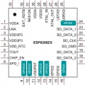
Pin Definitions

No. Pin Name Function Description
- 1 RST reset module
- 2 ADC A / D conversion result. Input voltage range of 0 ~ 1V, in the range: 0 to 1024
- 3 EN Chip Enable end, high effective
- 4 IO16 GPIO16; do wake deep sleep when receiving RST pin.
- 5 IO14 GPIO14; HSPI_CLK
- 6 IO12 GPIO12; HSPI_MISO
- 7 IO13 GPIO13; HSPI_MOSI; UART0_CTS
- 8 VCC 3.3V power supply
- 9 CS0 chip select
- 10 MISO output of the slave master input
- 11 IO9 SPI 9
- 12 IO10 GBIO10
- 13 MOSI Master Out Slave
- 14 SCLK clock
- 15 GND GND
- 16 IO15 GPIO15; MTDO; HSPICS; UART0_RTS
- 17 IO2 GPIO2; UART1_TXD
- 18 IO0 GPIO0
- 19 IO4 GPIO4
- 20 IO5 GPIO5
- 21 RXD UART0_RXD; GPIO3
- 22 TXD UART0_TXD; GPIO1
Pin Mode Configuration
Mode GPIO 15 GPIO0 GPIO_EN
- UART download mode: Low - Low - High
- Flash Boot Mode: Low - High - High
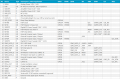
Signal sensitivity
| parameter | min. | typical | max. | unit |
|---|---|---|---|---|
| input frequency | 2412 | 2484 | mhz | |
| input resistor | 50 | Ω | ||
| input reflection | -10 | dB | ||
| PA output power on 72.2 Mbps | 14 | 15 | 16 | dbm |
| PA output power on 11b | 17.5 | 18.5 | 19.5 | dbm |
| sensitivity | ||||
| DSSS, 1Mbps | -98 | dBm | ||
| CCK, 11Mbps | -91 | dBm | ||
| 6 Mbps (1/2 BPSK) | -93 | dBm | ||
| 54 Mbps (3/4 64-QAM) | -75 | dBm | ||
| HT20, MCS7 (65 Mbps, 72.2 Mbps) | -72 | dBm | ||
| Adjacent suppression | ||||
| OFDM, 6 Mbps | 37 | dB | ||
| OFDM, 54 Mbps | 21 | dB | ||
| HT20, MCS0 | 37 | dB | ||
| HT20, MCS7 | 20 | dB |
Size and Mimension
- Dimensions ESP-12F SMD module is 16mm * 24mm * 3mm).
- The module uses a capacity of 4MB, packaged as SOP-210 mil of SPI Flash.
- Modules using a 3 DBi of PCB-board antenna.
LWH - PAD size (bottom) - pin pitch
- 16 mm 24 mm 3 mm - 0.9 mm x 1.7 mm - 2 mm
Function Description
MCU ESP8266EX built Tensilica L106 ultra-low power 32-bit micro MCU, with 16 compact mode, clocked at 80 MHz and supports 160 MHz, support for RTOS. Using the WiFi protocol stack is currently only 20% of MIPS, the other can be used for application development. MCU chip through the following interfaces and other parts of the work:
- Connection storage controller, it can also be used to access external code memory RAM / ROM Interface (iBus)
- Also connected to the data RAM memory controller interfaces (dBus)
- AHB interface to access the registers
Memory
Built-in SRAM and ROM - Auto body built ESP8266EX chip memory controller, comprising ROM and SRAM. MCU can access the storage controller iBus, dBus and AHB interface. These interfaces are accessible ROM or RAM unit, memory arbiter to determine the running order in the order of arrival. Based on the current Division I Demo SDK use SRAM, the user can remaining SRAM space: (next station mode, even after routed, heap + data area generally available around 36KB) RAM size <36kB not programmable ROM on ESP8266EX sheet Currently, users the program stored in the SPI Flash.
SPI Flash
- Current ESP8266EX chip SPI interface supports external Flash, a theoretical maximum support to 16 MB of SPI flash. At present, the module is 4MB of external SPI Flash.
- Recommendations Flash Capacity: 1 MB-16MB.
- Supported SPI mode: Standard SPI, Dual SPI, DIO SPI, QIO SPI, and Quad SPI. Note that you need to select the corresponding mode in the download tool when downloading firmware, or after downloading the program will not be run correctly.
Crystal
- Currently crystal 40M, 26M and 24M support, please pay attention to selecting the corresponding type of crystals in the download tool use. Crystal input and output of the applied determination of adjusted capacitors C1, C2 may be set to a fixed value, the value range in 6pF ~ 22pF, specific values need to be adjusted after the system test. Based on the current market situation in the mainstream of crystal, general 26Mhz oscillator input and output of the added capacitors C1, C2 in less than 10pF; general 40MHz crystal input and output capacitance added 10pF <C1, C2 <22pF.
- Optional precision crystal itself need to ± 10PPM. Crystal operating temperature -20 ° C- 85 ° C.
- Crystal position as close to the chip XTAL Pins (traces not too long), while crystal alignment to be wrapped up well shielded land.
- Crystal input and output traces can not punch alignment, that can not cross-layer. Crystal input and output traces can not cross, cross-layer cross too.
- Crystal input and output bypass capacitors placed left and right side close to the chip, please, try not to go on line.
- 4 layers beneath the crystal can not take the high-frequency digital signal, the best situation is below the crystal does not go any signal lines, paved TOP crystal surface area the better. Crystal sensitive devices around the crystal can not have magnetic induction devices, such as large inductors.
Interface
| Interface | Pins |
|---|---|
| HSPI Interface: External 4SPI Flash, display and MCU like | IO12 (MISO), IO13 (MOSI), IO14 (CLK), IO15 (CS) |
| PWM interface: the demo offers four PWM (to 8 users can expand their own way), can be used to control the color, lights, buzzers, relays and motors. | IO12 (R), IO15 (G), IO13 (B) |
| IR interface: IR Remote Control 4 interfaces implemented by software, interface NEC coding and modulation, demodulating, using 38KHz modulated carrier. | IO14 (IR_T), IO5 (IR_R) |
| ADC interface: It can be used to detect VDD3P3 (Pin3, Pin4) supply voltage and TOUT (Pin6) input voltage (not both). It can be used for sensor applications. | TOUT |
| I2C Interface: displays and other external sensors | IO14 (SCL), IO2 (SDA) |
| UART interface: Download: U0TXD + U0RXD or GPIO2 + U0RXD | UART0: TXD (U0TXD), RXD (U0RXD), IO15 (RTS), IO13 (CTS) UART1: IO2 (TXD) |
| UART interface: Communication (UART0): U0TXD, U0RXD, MTDO (U0RTS), MTCK (U0CTS) Debug: UART1_TXD (GPIO2) can be used as a print debug information. | UART0: TXD (U0TXD), RXD (U0RXD), IO15 (RTS), IO13 (CTS) UART1: IO2 (TXD) |
| UART interface: UART0 default on ESP8266EX power output will be some printed information. For sensitive applications, you can use the internal UART pin swapping function in initialization time, will U0TXD, U0RXD were exchanged with U0RTS, U0CTS. Admiral MTDO MTCK hardware connected to the corresponding external MCU serial communication. | UART0: TXD (U0TXD), RXD (U0RXD), IO15 (RTS), IO13 (CTS) UART1: IO2 (TXD) |
| I2S interface: Use main audio capture, processing and transmission. | I2S input: IO12 (I2SI_DATA); I2S input: IO13 (I2SI_BCK); I2S input: IO14 (I2SI_WS); I2S output: IO15 (I2SO_BCK); I2S output: IO3 (I2SO_DATA); I2S output: IO2 (I2SO_WS). |
ESP-12F for NodeMCU, D1-mini Pin Definition
- ESP-12F left side pin out
|
! Description | ESP8266 Internal | UART / IIC//SPI | Boot | ESP Relay Board |
|---|---|---|---|---|---|
| RST | Reset | RST | |||
| A0 | AD input, 0-3.3V | ADC | |||
| EN | |||||
| D0 |
|
GPIO16 | Status LED | ||
| D5 | I/O | GPIO14, MTMS |
|
DHT22 | |
| D6 | I/O | GPIO12 |
|
Relay 1 | |
| D7 | I/O | GPIO13, MTCK |
|
Relay 2 | |
| 3V3 | Power 3v3 | 3.3V |
- ESP-12F right side pin out
|
! Description | ESP8266 Internal | UART / IIC/SPI | Boot | ESP Relay Board |
|---|---|---|---|---|---|
| TX | Serial Send | GPIO1 |
|
Lead out | |
| RX | Serial Receive | GPIO3 |
|
Lead out | |
| D1 | I/O | GPIO5 |
|
Lead out | |
| D2 | I/O | GPIO4 |
|
Lead out | |
| D3 | I/O | GPIO0 |
|
BTN2 | |
| D4 | I/O | GPIO2 |
|
|
BTN1 |
| D8 | I/O | GPIO15 |
|
|
|
| G | GND | GND |
- All IO operational voltage is 3.3V, can handle 5V shortly
- except D0, all IO support interprut, PWM, I2C and 1-wire
extra gpio
pin

