Category:AC-DC circuits
AC - DC
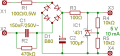
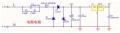
Capacitive power supply, less transformer need
X Rated capacitor 400 Volt, reference link


Chipless
01
02

03 - transformer (60:1 or so)
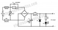
Basic Circuit
Basic Charger
Schematic
01
02
03

Working method
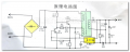
- 该电路由开关电源和输出电路两部分组成。
- 当接通电源后,220V交流通过D3整流,C1滤波.
- 通过电阻R1给三极管Q1提供基极启动电流,使Q1开始导通,其集电极电流Ic线性增长,在L2中感应出使Q1基极为正、发射极为负的正反馈电压,通过C3和R3,送到Q1基极,使Q1迅速饱和。与此同时,感应电动势给电容C3充电,随着C3充电电压升高,Q1基极电位逐渐下降,Ic开始减小,在L2中感应出使Q1基极为负,发射极为正的电压,使Q1迅速截止,完成一个振荡周期,在Q1截止期间,在L3绕组感应出一个5V左右的交流电压。此后,C3逐渐放电,Q1基极电压逐渐升高,从而开始第二个周期,不断循环。
- L3输出电压经D6整流、C4滤波后通过USB座给负载供电。LED1和R5组成输出指示电路。
- Z1、IC1、Q2等组成取样比较电路,检查输出电压的高低。当负载变轻或电源电压升高等原因导致输出电压升高时,Z1击穿,IC1中发光二级管电流增大,IC1中光敏三极管电流增大。L2反馈绕组中的感应电压经IC1中的光敏三极管到Q2基极,Q2基极电流增大,集电极电流增大,Q1基极电流减小,集电极电流减小,负载能力变小,从而导致输出电压降低。当输出电压降低后,Q2取样后又会截止,Q1的负载能力变强,输出电压升高,这样起到自动稳压作用。D5为L2绕组输出电压整流二极管,C2为滤波电容。
- 本电路设计有过流过载保护功能。当负载过载或者短路时,Q1的集电极电流增大,Q1的发射极电阻R2上产生较高的压降,这个过载或者短路产生的高电压经过R4让Q2饱和导通,从而让Q1截止,停止输出,防止过载损坏。因此,改变R2的大小,可改变负载能力。如果将输出电流减小,可将R2改大。如果将输出电流改大,可将R2改小。注意:R2改小将增大Q1烧坏的可能性。如果需要大电流输出,建议更换Q1为13003或者13007中大功率三极管。
Working Method 02
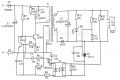
- 本电路包括典型开关稳压电源的各组成单元。
- 低频整流滤波电路由D2、C1、R1组成,将220V交流转化为300V非稳直流,R1兼做保险的功能;
- 启动电阻R7为开关管Q1提供启动电流;
- 开关变压器T1的初级绕组1-2,反馈绕组4-5,正反馈网络R6、C2及开关管组成自激振荡电路;
- Q2为分流管,脉冲宽度调制及各种保护均通过它对开关管基极电流的分流来实现;
- R2、R3组成过流保护电路;
- D1、C3、R4组成开关管集电极尖峰电压吸收电路;
- D3、C4组成整流滤波电路,为光耦供电;
- C5对脉宽调制信号起平滑作用,杜绝分流管提前分流;
- 开关变压器的次级绕组6-10产生的感应电压经过续流管D5整流,C7滤波输出直流电;
- R13和LED组成输出电源指示灯电路;
- R11、12组成取样电路;基准电压由TL431产生;误差信号经过光耦U1隔离传输到脉宽调制电路实现对开关管的精确控制,从而输出稳定直流电压。
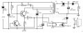
Working method 03 CN
功能描述:本电源按优质进囗电电路设计,能将220V交流电转化为5V稳定直流电输出,由正采用TL431精稳压,0一800mA内电压非常定。输出电流最人可以达到850mA。输入采用中规插头,输出为USB座,可以做手机直充、单片机实验、各种小制作等的供电设各。
原理简介:本电路包括典型开关稳压电源的各组成单元。
- 低频整流滤波电路D2, C1, R1组成,将220V交流转化为300V非稳直流,R1兼做保险的功能;
- 启动电阻R7为开关管QI提供启动电流:
- 开关变压器Tl的初级绕组1一2,反馈绕组4一5,正反馈网络R6、C2及开关管组成自激振电路;
- Q2为分流管,脉冲宽度调制及各种保护均通过它对开关管基极电流的分流来实现;
- R2、R3组成过流保护电路;
- D1、C3、R4组成开关管集电极尖峰电压吸收电路;
- D3、C4组成整流滤波电路,为光耦供电;
- C5对脉宽调制信号起平滑作用,杜绝分流管提前分流;
- 开关变压器的次级绕组6一10产生的感应电压经过续流管D5整流,C7滤波输出直流电;
- R13和LED组成输出电源指示灯电路;
- R11、12组成取样电路;
- 基准电压由TL431产生;误差信号经过光耦旧隔离传输到脉宽调制电路实现对开关管的精确控制,从而输出稳定直流电压。
装配注意事项:
- 1. 所有元件均紧贴电路板表面安装。
- 2. 剪脚时不要用力拉动引脚,这样容易使焊盘与铜箔断裂而开路。
- 3. 取样电阻R11、R12需用精密电阻。
- 4·注意光耦、电解电容、二极管、三极管的方向不要装反。
Working method 03 EN
Function description: This power supply is designed according to the high-quality electric circuit, which can convert 220V AC into 5V stable DC output. It is regulated by TL431, and the voltage is very fixed within 0-800mA. The output current can reach 850mA. The input adopts the middle gauge plug, and the output is a USB socket. It can be used as a power supply for direct charging of mobile phones, single-chip experiments, and various small productions.
Principle introduction: This circuit includes the components of a typical switching regulator power supply.
- Low-frequency rectification and filtering circuit D2, C1, R1, convert 220V AC into 300V unsteady DC, R1 also serves as insurance function;
- The starting resistor R7 provides the starting current for the switching transistor QI:
- The primary winding 1 - 2 of the switching transformer T1, the feedback winding 4 - 5, the positive feedback network R6, C2 and the switching tube form a self-exciting circuit;
- Q2 is a shunt tube, pulse width modulation and various protections are realized by its shunting of the base current of the switch tube;
- R2 and R3 form an overcurrent protection circuit;
- D1, C3, R4 form the collector peak voltage absorption circuit of the switch tube;
- D3, C4 form a rectification and filtering circuit to supply optocoupler;
- C5 smoothes the pulse width modulation signal to prevent the shunt tube from being shunted in advance;
- The induced voltage generated by the secondary winding 6-10 of the switching transformer is rectified by the freewheeling tube D5, and the C7 filter outputs the direct current;
- R13 and LED form the output power indicator circuit;
- R11, 12 constitute a sampling circuit;
- The reference voltage is generated by TL431; the error signal is transmitted to the pulse width modulation circuit through the optocoupler's old isolation to achieve precise control of the switching tube, thereby outputting a stable DC voltage.
Assembly notes:
- 1. All components are mounted against the surface of the board.
- 2. Do not pull the pins hard when cutting the feet. This will easily break the pads and the copper foil and open the way.
- 3. Precision resistors are required for the sampling resistors R11 and R12.
- 4. Note that the direction of the optocoupler, electrolytic capacitor, diode, and triode should not be reversed.
Power supply of HLW8012
- More non-isoated power module refer to AC-DC
In order to match the resistance sampling method (ie, direct sampling signal from the grid, non-isolated), the power supply circuit must be non-isolated power supply, non-isolated power supply in two ways: AC-DC non-isolated power supply, The comparison is as follows:
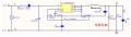
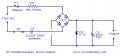
LNK304 designed AC-DC non-isolated power supply
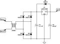
Resistive buck power supply
- LNK304 designed AC-DC non-isolated power supply
The use of LNK304 designed AC-DC non-isolated power supply, L and N, respectively, is the AC line and the zero line to zero line as a ground. This circuit does not need transformer, regulator 5V, can provide about 150mA current, to ensure that AC85V ~ 265V AC range, to achieve a stable voltage output, ripple is also very small, about 50mV. This power supply provides operating voltage for all modules.
- Resistive buck power supply
After the regulator capacitor C1 step-down, the diode rectifier, the use of 1N4749 power down to 24V, and then through the regulator chip 78L05 output power stabilized at 5V, to provide power to the HLW8012, 24V for driving the relay. If the choice of 12V relay, then 1N4749 need to be changed to 1N4742, but the safety capacitor C1 need to be changed to 1uF capacitor to improve the drive current.
Reference
This category currently contains no pages or media.