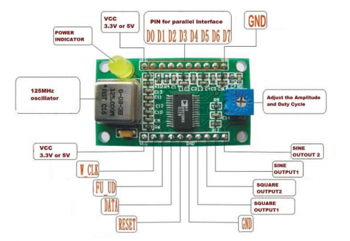
AD9850 Module DDS Signal Generator V2
Pin Maps
Pins Definitions
| Symbol | Type | Functions |
|---|---|---|
| VCC | P | This is a voltage supply pin. 3.3V or 5V power input |
| GND | P | This is a ground pin. |
| W_CLK | I | Word Load Clock. This clock is used to load the parallel or serial frequency/phase/control words |
| FQ_UD | I | Frequency Update. On the rising edge of this clock, the DDS will update to the frequency (or phase) loaded in the data input register, it then resets the pointer to Word 0 |
| DATA | I | D7, Serial Load |
| RESET | I | Reset. This is the master reset function; when set high it clears all registers (except the input register) and the DAC output will go to Cosine 0 after additional clock cycles |
| D0–D7 | I | 8-Bit Data Input. This is the 8-bit data port for iteratively loading the 32-bit frequency and 8-bit phase/28–25 control word. D7 = MSB; D0 = LSB. D7 (Pin 25) also serves as the input pin for the 40-bit serial data word. |
| Square Wave Ouput1 | O | This is the comparator’s true output |
| Square Wave Ouput2 | O | This is the comparator’s complement output. |
| Sine Wave Ouput1 | O | Analog Current Output of the DAC. |
| Since Wave Ouput2 | O | The Complementary Analog Output of the DAC. |
Software Description
The AD9850 contains a 40-bit register that is used to program the 32-bit frequency control word, the 5-bit phase modulation word and the power-down function. This register can be loaded in a parallel or serial mode.
In the parallel load mode, the register is loaded via an 8-bit bus; the full 40-bit word requires five iterations of the 8-bit word. The W_CLK and FQ_UD signals are used to address and load the registers. The rising edge of FQ_UD loads the (up to) 40-bit control data word into the device and resets the address pointer to the first register. Subsequent W_CLK rising edges load the 8-bit data on words [7:0] and move the pointer to the next register. After five loads,
W_CLK edges are ignored until either a reset or an FQ_UD rising edge resets the address
pointer to the first register.
In serial load mode, subsequent rising edges of W_CLK shift the 1-bit data on Lead 25 (D7) through the 40 bits of programming information. After 40 bits are shifted through, an FQ_UD pulse is required to update the output frequency (or phase).
Arduino Demo Code
Using digital pins 8 through 11, proto shield installed on the UNO. Pin 8 to CLK, 9 to FQ, 10 to DATA, and 11 to RST.
 #define W_CLK 8       // Pin 8 - connect to AD9850 module word load clock pin (CLK)
 #define FQ_UD 9       // Pin 9 - connect to freq update pin (FQ)
 #define DATA 10       // Pin 10 - connect to serial data load pin (DATA)
 #define RESET 11      // Pin 11 - connect to reset pin (RST).

 #define pulseHigh(pin) {digitalWrite(pin, HIGH); digitalWrite(pin, LOW); }

 // transfers a byte, a bit at a time, LSB first to the 9850 via serial DATA line
void tfr_byte(byte data)
{
  for (int i=0; i<8; i++, data>>=1) {
    digitalWrite(DATA, data & 0x01);
    pulseHigh(W_CLK);   //after each bit sent, CLK is pulsed high
  }
}

 // frequency calc from datasheet page 8 = <sys clock> * <frequency tuning word>/2^32
void sendFrequency(double frequency) {
  int32_t freq = frequency * 4294967295/125000000;  // note 125 MHz clock on 9850
  for (int b=0; b<4; b++, freq>>=8) {
    tfr_byte(freq & 0xFF);
  }
  tfr_byte(0x000);   // Final control byte, all 0 for 9850 chip
  pulseHigh(FQ_UD);  // Done!  Should see output
}

void setup() {
 // configure arduino data pins for output
  pinMode(FQ_UD, OUTPUT);
  pinMode(W_CLK, OUTPUT);
  pinMode(DATA, OUTPUT);
  pinMode(RESET, OUTPUT);

  pulseHigh(RESET);
  pulseHigh(W_CLK);
  pulseHigh(FQ_UD);  // this pulse enables serial mode - Datasheet page 12 figure 10
}

void loop() {
  sendFrequency(10.e6);  // freq
  while(1);
}
Setting the output frequency
The output frequency is set by calculating a 40-bit turning word and loading it to the DDS, either via a 3-wire serial bus or an 8-bit parallel bus. The 40-bit word is comprised of 32-bits of phase and frequency information and a further 8-bit, 3-bits that set specific operating (and factory test) modes of the DDS - it is these 3-bits that cause problems when trying to use AD9851 code with the AD9850- and 5-bits of phase information. For simplicity, I set all of these bits to 0. The datasheet gives the following equation to calculate the turning word
This translates into C++ as
unsigned long tuning_word = (frequency * pow(2, 32)) / DDS_CLOCK;
using floating point maths. Or as
Unsigned long tuning_word = (frequency * 4294967296LL) / DDS_CLOCK;
using integer maths. In theory, integer maths should be slightly faster and more accurate as the required frequency increases, in practice I find either method fast enough and accurate enough up to 30MHz, frequency errors are due to the poor stability of the reference oscillator on the DDS module. Calculating the turning word and writing it to the DDS module can them be wrapped up in a single function taking the required frequency as its sole parameter
void SetFrequency(unsigned long frequency)
{
  unsigned long tuning_word = (frequency * pow(2, 32)) / DDS_CLOCK;
  digitalWrite (LOAD, LOW);

  shiftOut(DATA, CLOCK, LSBFIRST, tuning_word);
  shiftOut(DATA, CLOCK, LSBFIRST, tuning_word >> 8);
  shiftOut(DATA, CLOCK, LSBFIRST, tuning_word >> 16);
  shiftOut(DATA, CLOCK, LSBFIRST, tuning_word >> 24);
  shiftOut(DATA, CLOCK, LSBFIRST, 0x0);

  digitalWrite (LOAD, HIGH);
}

