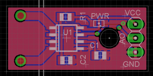
Eagle Design Checklist
1. Schematic
- Design all the packages that you will need in the design
- Run the ERC check
2. Board Design
The structure design
- Design the board shape generally in layer "dimension"
- And add installation holes if you have AFTER layout design
Layout design
Place components
- Set the main zones: digital signal area, analog signal area, power driving area
- Make sure the relevant components stay close, crystal should stay close to the one who use it.
- Concern the sensitive components: temperature sensitive, humidity sensitive, metal shield compoents etc
- Connectors should stay close to the edge of the board.
DRC and Autorouter
- Setup the DRC, for large size board, this can all keep default, for small small, only change "coper/dimension" in "distance" to 14 mil, and "minimium drill" "in sizes" to 14 mil.
- Use 45 degree trace instead of 90, do not make a loop circuit
- Run the autorouter
- Check the width for main power trace and large current flow trace, make sure it can handle the large current. for example, the large current flow on ACS712 sensor module, current up to 20A.
- If necessary, add testing point on important signal trace
- Cover with GND copper plane, and reset plane
Text
- Run "normalize-text.ulp" ULP to normalize all the text, adjust position
- Add extra words, descriptions, pins defintion in "tplace" layer (or "bplace").
- Make sure the text is not over the vias, as it won't print on it.
Check
- Rund the DRC check, make sure no "overlap", such mistakes.
3. Export
- If this is a panelize file, run "panelize" command in the tool menu, then tplace and bplace with copy to layer 125 and 126, and won't change value anymore
- run CAM Process job: Excellon and gerber274x file, for gerber274x, you should carefully select tplace, bplace, tname, bnames, tvalues, etc all these silk print text carefully for your board.
