Eagle Export
BOM
Coordinate
Gerber
These are my notes on creating a Gerber file from Eagle CadSoft.
Run gerber274x.cam for main gerber files
- open CAM processor = File | Cam Processor
- open CAM Processor , job file = File | Open | Job ...
- click "Process Job" and select "gerber274x.cam", in this step, if you panelizing your file, you should not use the 25 tNames layer anymore, but use 125 layer instead.
- you should have the similar setting like picture below, but you may have more if you have SMD parts on the bottom side, since we only have parts on the top side in this case.
Check the exported file according to the Gerber file extension of Eagle on this page.
- Review
Adding a second silk screen (Optional)
If you look at the tabs, you will see that you don’t have a file for silk screen bottom. For simple boards, the silk screen is usually on the top layer so that you don’t need the bottom. Some of the cheap circuit board manufacturers don’t even allow bottom silk screen.
But if you need silk screen on bottom layer as well, follow these steps:
- Click “Add”
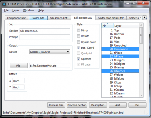
- Change Section to something like “Silk Screen SOL”
- Change File to “%N.pls”
- Deselect all layers
- Select layers 20 “Dimension”, 22 “bPlace” and 26 “bNames”
- There you go.
- The above options can also be found on gerb274x-4layers.cam
Run Excellons for hole files
- Repeat the step from 1-4,but this time run "excellon.cam" work。
Zip and check
- now you have all the gerber files under the fold, zip it.
- check the zipped gerber file by pantalogix tool to see if any forgot things or error


